


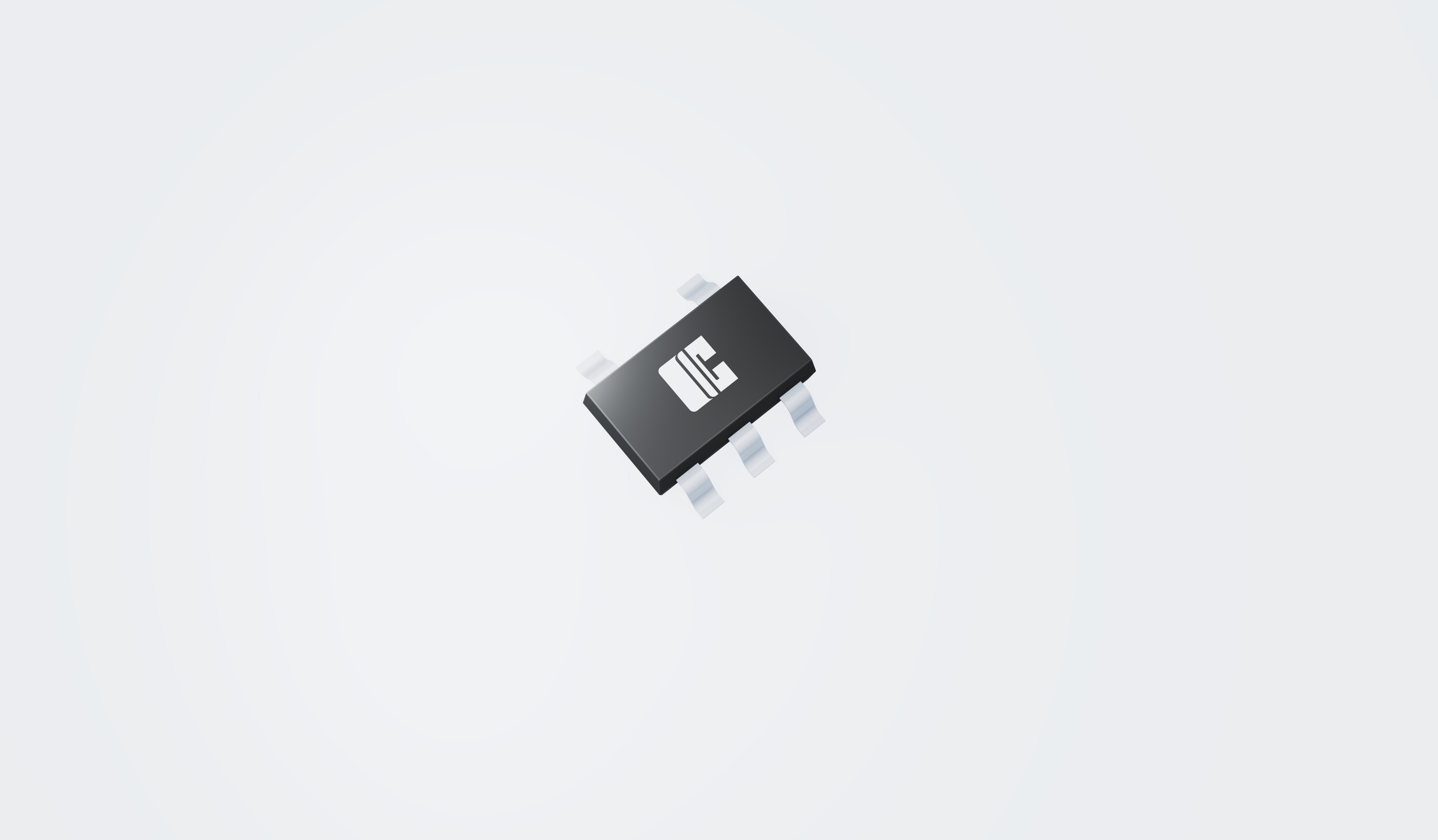
供給電圧範囲:
AiP74HC73: 2V~6V
AiP74HCT73: 4.5V~5.5V
入力レベル:
AiP74HC73: CMOSレベル
AiP74HCT73: TTLレベル
温度範囲:-40℃~+125℃
パッケージ情報: DIP14/SOP14/TSSOP14
-1769477122jv1iL1kpji.jpg)
-17694772923alulrrexR.jpg)
The AiP74HC/HCT196 is a presettable decade and binary counter. Output Q0 is connected to input CP1(—) for BCD count. Output Q3 is connected to input CP0(—) for bi-quinary count. In the counting modes, state changes are initiated by the falling edge of the clock.
詳細-1769561865c92qFRf2EX.jpg)
The AiP74HC/HCT196 is a presettable decade and binary counter. Output Q0 is connected to input CP1(—) for BCD count. Output Q3 is connected to input CP0(—) for bi-quinary count. In the counting modes, state changes are initiated by the falling edge of the clock.
詳細-17695651472X0l1ZKkjw.jpg)
The AiP74HC/HCT240 is an 8-bit inverting buffer/line driver with 3-state outputs. The device can be used as two 4-bit buffers or one 8-bit buffer. The device features two output enables (1OE(—) and 2OE(—)), each controlling four of the 3-state outputs. A HIGH on nOE(—) causes the outputs to assume a high-impedance OFF-state. Inputs include clamp diodes that enable the use of current limiting resistors to interface inputs to voltages in excess of VCC
詳細-1769565273c5wHTNtUYA.jpg)
The AiP74HC/HCT240 is an 8-bit inverting buffer/line driver with 3-state outputs. The device can be used as two 4-bit buffers or one 8-bit buffer. The device features two output enables (1OE(—) and 2OE(—)), each controlling four of the 3-state outputs. A HIGH on nOE(—) causes the outputs to assume a high-impedance OFF-state. Inputs include clamp diodes that enable the use of current limiting resistors to interface inputs to voltages in excess of VCC.
詳細-1769566649Hjv3Ld3Ug8.jpg)
The AiP74HC/HCT241 is an 8-bit buffer/line driver with 3-state outputs. The device can be used as two 4-bit buffers or one 8-bit buffer. The device features two output enables (1OE(—) and 2OE), each controlling four of the 3-state outputs. A HIGH on 1OE(—) or LOW on 2OE causes the associated outputs to assume a high-impedance OFF-state. Inputs include clamp diodes. This enables the use of current limiting resistors to interface inputs to voltages in excess of VCC. The AiP74HC/HCT241 device features reduced input threshold levels to allow interfacing to TTL logic levels.
詳細-1769566724eNN8rnmjcg.jpg)
The AiP74HC/HCT241 is an 8-bit buffer/line driver with 3-state outputs. The device can be used as two 4-bit buffers or one 8-bit buffer. The device features two output enables (1OE(—) and 2OE), each controlling four of the 3-state outputs. A HIGH on 1OE(—) or LOW on 2OE causes the associated outputs to assume a high-impedance OFF-state. Inputs include clamp diodes. This enables the use of current limiting resistors to interface inputs to voltages in excess of VCC. The AiP74HC/HCT241 device features reduced input threshold levels to allow interfacing to TTL logic levels.
詳細-1769567103SsK0oyxbSC.jpg)
The AiP74HC/HCT243 are quad bus transceivers featuring non-inverting 3-state bus compatible outputs in both send and receive directions. They are designed for 4-line asynchronous 2-way data communications between data buses. The output enable inputs (OE(—)A and OEB) can be used to isolate the buses.
詳細-17695672826qDdUSaZJ5.jpg)
The AiP74HC/HCT243 are quad bus transceivers featuring non-inverting 3-state bus compatible outputs in both send and receive directions. They are designed for 4-line asynchronous 2-way data communications between data buses. The output enable inputs (OE(—)A and OEB) can be used to isolate the buses.
詳細-1769580684JlE5FmyPtH.jpg)
The AiP74HC/HCT244 is an 8-bit buffer/line driver with 3-state outputs. The device can be used as two 4-bit buffers or one 8-bit buffer. The device features two output enables (1OE(—) and 2OE(—)), each controlling four of the 3-state outputs. A HIGH on nOE(—) causes the outputs to assume a high-impedance OFF-state. Inputs include clamp diodes that enable the use of current limiting resistors to interface inputs to voltages in excess of VCC.
詳細-1769580769K3ENbayJ48.jpg)
The AiP74HC/HCT244 is an 8-bit buffer/line driver with 3-state outputs. The device can be used as two 4-bit buffers or one 8-bit buffer. The device features two output enables (1OE(—) and 2OE(—)), each controlling four of the 3-state outputs. A HIGH on nOE(—) causes the outputs to assume a high-impedance OFF-state. Inputs include clamp diodes that enable the use of current limiting resistors to interface inputs to voltages in excess of VCC.
詳細
AiP74HC245は、3ステート出力を備えた8ビットトランシーバです。このデバイスは、出力イネーブル(OE — )と送受信方向制御用のDIR(DIR)を備えています。OE — がHIGHになると、出力は高インピーダンスのOFF状態になります。入力にはクランプダイオードが内蔵されており、これにより、VCCを超える電圧への入力インターフェースに電流制限抵抗を使用することができます。
詳細-1769580927USpKelMtOh.jpg)
The AiP74HC/HCT247 feature active-low outputs designed for driving common-anode LEDs or incandescent indicators directly. Display patterns for BCD input counts above 9 are unique symbols to authenticate input conditions.
詳細
-1769581396d02IDWKiNO.jpg)
The AiP74HC/HCT248 feature active-low outputs designed for driving common-cathode LEDs or incandescent indicators directly. Display patterns for BCD input counts above 9 are unique symbols to authenticate input conditions.
詳細
-1769581517LXS5QhMDcc.jpg)
The AiP74HC/HCT251 is an 8-bit multiplexer with eight binary inputs (I0 to I7), three select inputs (S0 to S2) and an output enable input (OE(—)). The select inputs select one of the eight binary inputs and route it to the complementary outputs (Y and Y(—)). A HIGH on OE(—) causes the outputs to assume a high-impedance OFF-state. Inputs include clamp diodes that enable the use of current limiting resistors to interface inputs to voltages in excess of VCC.
詳細
-17695817539bWrX6JSIL.jpg)
The AiP74HC/HCT251 is an 8-bit multiplexer with eight binary inputs (I0 to I7), three select inputs (S0 to S2) and an output enable input (OE(—)). The select inputs select one of the eight binary inputs and route it to the complementary outputs (Y and Y(—)). A HIGH on OE(—) causes the outputs to assume a high-impedance OFF-state. Inputs include clamp diodes that enable the use of current limiting resistors to interface inputs to voltages in excess of VCC.
詳細
-17695828134yuhMBvsAP.jpg)
The AiP74HC/HCT259 is an 8-bit addressable latch. The device features four modes of operation. In the addressable latch mode, data on the D input is written into the latch addressed by the inputs A0 to A3. The addressed latch will follow the data input, non-addressed latches will retain their previous states. In memory mode, all latches retain their previous states and are unaffected by the data or address inputs. In the 3-to-8 decoding or demultiplexing mode, the addressed output follows the D input and all other outputs are LOW. In the reset mode, all outputs are forced LOW and unaffected by the data or address inputs. Inputs include clamp diodes. This enables the use of current limiting resistors to interface inputs to voltages in excess of VCC.
詳細
-1769583039uoKphYEKUM.jpg)
The AiP74HC/HCT259 is an 8-bit addressable latch. The device features four modes of operation. In the addressable latch mode, data on the D input is written into the latch addressed by the inputs A0 to A3. The addressed latch will follow the data input, non-addressed latches will retain their previous states. In memory mode, all latches retain their previous states and are unaffected by the data or address inputs. In the 3-to-8 decoding or demultiplexing mode, the addressed output follows the D input and all other outputs are LOW. In the reset mode, all outputs are forced LOW and unaffected by the data or address inputs. Inputs include clamp diodes. This enables the use of current limiting resistors to interface inputs to voltages in excess of VCC.
詳細-1769588143JEbaD36zeV.jpg)
The AiP74HC/HCT266 contains four independent 2-input XNOR Gates with open-drain outputs
詳細
-1769588224qNmEV3D0Em.jpg)
The AiP74HC/HCT266 contains four independent 2-input XNOR Gates with open-drain outputs
詳細
-1769588337DfFRMq62mq.jpg)
The AiP74HC/HCT273 is an octal positive-edge triggered D-type flip-flop. The device features clock (CP) and master reset (MR(—)) inputs. The outputs Qn will assume the state of their corresponding Dn inputs that meet the set-up and hold time requirements on the LOW-to-HIGH clock (CP) transition. A LOW on MR(—) forces the outputs LOW independently of clock and data inputs. Inputs include clamp diodes. This enables the use of current limiting resistors to interface inputs to voltages in excess of VCC.
詳細
-1769588427hLq11mzSQO.jpg)
The AiP74HC/HCT273 is an octal positive-edge triggered D-type flip-flop. The device features clock (CP) and master reset (MR(—)) inputs. The outputs Qn will assume the state of their corresponding Dn inputs that meet the set-up and hold time requirements on the LOW-to-HIGH clock (CP) transition. A LOW on MR(—) forces the outputs LOW independently of clock and data inputs. Inputs include clamp diodes. This enables the use of current limiting resistors to interface inputs to voltages in excess of VCC.
詳細
-1769588560N4RhJlBrQa.jpg)

-1769588664udNSattNrA.jpg)

-1769588807i1sTBUUs1A.jpg)
The AiP74HC/HCT280 is a 9-bit parity generator or checker. Both even and odd parity outputs are available. The even parity output (PE) is HIGH when an even number of data inputs (I0 to I8) is HIGH. The odd parity output (PO) is HIGH when an odd number of data inputs are HIGH. Expansion to larger word sizes is accomplished by tying the even outputs (PE) of up to nine parallel devices to the final stage data inputs. Inputs include clamp diodes. It enables the use of current limiting resistors to interface inputs to voltages in excess of VCC.
詳細
-1769588968uMA3dyeXqw.jpg)
The AiP74HC/HCT280 is a 9-bit parity generator or checker. Both even and odd parity outputs are available. The even parity output (PE) is HIGH when an even number of data inputs (I0 to I8) is HIGH. The odd parity output (PO) is HIGH when an odd number of data inputs are HIGH. Expansion to larger word sizes is accomplished by tying the even outputs (PE) of up to nine parallel devices to the final stage data inputs. Inputs include clamp diodes. It enables the use of current limiting resistors to interface inputs to voltages in excess of VCC.
詳細
-17695891743DCQjx0JnJ.jpg)
The AiP74HC/HCT283 adds two 4-bit binary words (An plus Bn) plus the incoming carry (CIN). The binary sum appears on the sum outputs (S1 to S4) and the out-going carry (COUT) according to the equation: CIN+(A1+B1)+2(A2+B2)+4(A3+B3)+8(A4+B4)==S1+2S2+4S3+8S4+16COUT Where (+) = plus. Due to the symmetry of the binary add function, the AiP74HC/HCT283 can be used with either all active HIGH operands (positive logic) or all active LOW operands (negative logic). In case of all active LOW operands the results S1 to S4 and COUT should be interpreted also as active LOW. With active HIGH inputs, CIN must be held LOW when no carry in is intended. Interchanging inputs of equal weight does not affect the operation, thus CIN, A1, B1 can be assigned arbitrarily to pins 5, 6, 7, etc.
詳細
-1769589272kF6YGhBXse.jpg)
The AiP74HC/HCT283 adds two 4-bit binary words (An plus Bn) plus the incoming carry (CIN). The binary sum appears on the sum outputs (S1 to S4) and the out-going carry (COUT) according to the equation: CIN+(A1+B1)+2(A2+B2)+4(A3+B3)+8(A4+B4)==S1+2S2+4S3+8S4+16COUT Where (+) = plus. Due to the symmetry of the binary add function, the AiP74HC/HCT283 can be used with either all active HIGH operands (positive logic) or all active LOW operands (negative logic). In case of all active LOW operands the results S1 to S4 and COUT should be interpreted also as active LOW. With active HIGH inputs, CIN must be held LOW when no carry in is intended. Interchanging inputs of equal weight does not affect the operation, thus CIN, A1, B1 can be assigned arbitrarily to pins 5, 6, 7, etc.
詳細
-1769589411n7oKPkI9RN.jpg)
The AiP74HC/HCT365 is a hex buffer/line driver with 3-state outputs controlled by the output enable inputs (OE(—)n). A HIGH on OE(—)n causes the outputs to assume a high impedance OFF-state. Inputs include clamp diodes. This enables the use of current limiting resistors to interface inputs to voltages in excess of VCC.
詳細
-1769589498DNQMdughcL.jpg)
The AiP74HC/HCT365 is a hex buffer/line driver with 3-state outputs controlled by the output enable inputs (OE(—)n). A HIGH on OE(—)n causes the outputs to assume a high impedance OFF-state. Inputs include clamp diodes. This enables the use of current limiting resistors to interface inputs to voltages in excess of VCC.
詳細
AiP74HC164 は、8 ビットのシリアル入力/パラレル出力シフト レジスタです。 e AiP74HC/HCT164は、8ビットのシリアル入力/パラレル出力シフトレジスタです。このデバイスは2つのシリアルデータを備えています。AiP74HC/HCT164は、8ビットのシリアル入力/パラレル出力シフトレジスタです。このデバイスは2つのシリアルデータを備えています。入力 (DSA および DSB)、8 つのパラレル データ出力 (Q0 ~ Q7)。 入力 (DSA および DSB)、8 つのパラレル データ出力 (Q0 ~ Q7)。
詳細-1769661600fcHl8bBOZv.jpg)
The AiP74HC/HCT366 is a hex inverting buffer/line driver with 3-state outputs controlled by the output enable inputs (OE(—)n). A HIGH on OE(—)n causes the outputs to assume a high impedance OFF-state. Inputs include clamp diodes. This enables the use of current limiting resistors to interface inputs to voltages in excess of VCC.
詳細
-1769661665IzSFDEeSEW.jpg)
The AiP74HC/HCT366 is a hex inverting buffer/line driver with 3-state outputs controlled by the output enable inputs (OE(—)n). A HIGH on OE(—)n causes the outputs to assume a high impedance OFF-state. Inputs include clamp diodes. This enables the use of current limiting resistors to interface inputs to voltages in excess of VCC.
詳細-1769661812uVo0ixlIjn.jpg)
The AiP74HC/HCT367 is a hex buffer/line driver with 3-state outputs controlled by the output enable inputs (nOE(—)). A HIGH on nOE(—) causes the outputs to assume a high impedance OFF-state. Inputs include clamp diodes. This enables the use of current limiting resistors to interface inputs to voltages in excess of VCC.
詳細-1769661886g7lAkpry5r.jpg)
The AiP74HC/HCT367 is a hex buffer/line driver with 3-state outputs controlled by the output enable inputs (nOE(—)). A HIGH on nOE(—) causes the outputs to assume a high impedance OFF-state. Inputs include clamp diodes. This enables the use of current limiting resistors to interface inputs to voltages in excess of VCC.
詳細
-1769662011afD5EIQjx7.jpg)
The AiP74HC/HCT373 is an octal D-type transparent latch with 3-state outputs. The device features latch enable (LE) and output enable (OE(—)) inputs. When LE is HIGH, data at the inputs enter the latches. In this condition the latches are transparent, a latch output will change each time its corresponding D-input changes. When LE is LOW the latches store the information that was present at the inputs a set-up time preceding the HIGH-to-LOW transition of LE. A HIGH on OE(—) causes the outputs to assume a high-impedance OFF-state. Operation of the OE(—) input does not affect the state of the latches. Inputs include clamp diodes. This enables the use of current limiting resistors to interface inputs to voltages in excess of VCC.
詳細
-17696620848rQMTSEl4A.jpg)
The AiP74HC/HCT373 is an octal D-type transparent latch with 3-state outputs. The device features latch enable (LE) and output enable (OE(—)) inputs. When LE is HIGH, data at the inputs enter the latches. In this condition the latches are transparent, a latch output will change each time its corresponding D-input changes. When LE is LOW the latches store the information that was present at the inputs a set-up time preceding the HIGH-to-LOW transition of LE. A HIGH on OE(—) causes the outputs to assume a high-impedance OFF-state. Operation of the OE(—) input does not affect the state of the latches. Inputs include clamp diodes. This enables the use of current limiting resistors to interface inputs to voltages in excess of VCC.
詳細
-1769662189tByqUd3ba6.jpg)
The AiP74HC/HCT374 is an octal positive-edge triggered D-type flip-flop with 3-state outputs. The device features a clock (CP) and output enable (OE(—)) inputs. The flip-flops will store the state of their individual D-inputs that meet the set-up and hold time requirements on the LOW-to-HIGH clock (CP) transition. A HIGH on OE(—) causes the outputs to assume a high-impedance OFF-state. Operation of the OE(—) input does not affect the state of the flip-flops. Inputs also include clamp diodes, this enables the use of current limiting resistors to interface inputs to voltages in excess of VCC. The AiP74HCT374 features reduced input threshold levels to allow interfacing to TTL logic levels.
詳細
-17696622697EMzfG9dIn.jpg)
The AiP74HC/HCT374 is an octal positive-edge triggered D-type flip-flop with 3-state outputs. The device features a clock (CP) and output enable (OE(—)) inputs. The flip-flops will store the state of their individual D-inputs that meet the set-up and hold time requirements on the LOW-to-HIGH clock (CP) transition. A HIGH on OE(—) causes the outputs to assume a high-impedance OFF-state. Operation of the OE(—) input does not affect the state of the flip-flops. Inputs also include clamp diodes, this enables the use of current limiting resistors to interface inputs to voltages in excess of VCC. The AiP74HCT374 features reduced input threshold levels to allow interfacing to TTL logic levels.
詳細
-1769662412SG4QV6cdsI.jpg)
-1769662474Aom47PAeLF.jpg)
-1769750250nL9pwru2P8.jpg)
The AiP74HC/HCT540 is an 8-bit inverting buffer/line driver with 3-state outputs. The device features two output enables (OE(—)1 and OE(—)2). A HIGH on OE(—)n causes the outputs to assume a high-impedance OFF-state. Inputs include clamp diodes. This enables the use of current limiting resistors to interface inputs to voltages in excess of VCC.
詳細-1769750319bwzB0cyHnT.jpg)
The AiP74HC/HCT540 is an 8-bit inverting buffer/line driver with 3-state outputs. The device features two output enables (OE(—)1 and OE(—)2). A HIGH on OE(—)n causes the outputs to assume a high-impedance OFF-state. Inputs include clamp diodes. This enables the use of current limiting resistors to interface inputs to voltages in excess of VCC.
詳細-17697526006OGygh48Qd.jpg)
The AiP74HC/HCT541 is an octal non-inverting buffer/line driver with 3-state outputs. The device features two output enables (OE(—)1 and OE(—)2). A HIGH on OE(—)n causes the outputs to assume a high-impedance OFF-state. Inputs include clamp diodes that enable the use of current limiting resistors to interface inputs to voltages in excess of VCC.
詳細-1769752677Y3NMkHUdsL.jpg)
The AiP74HC/HCT541 is an octal non-inverting buffer/line driver with 3-state outputs. The device features two output enables (OE(—)1 and OE(—)2). A HIGH on OE(—)n causes the outputs to assume a high-impedance OFF-state. Inputs include clamp diodes that enable the use of current limiting resistors to interface inputs to voltages in excess of VCC.
詳細-1769756121c2UdSoFC7Z.jpg)
The AiP74HC/HCT563 is an 8-bit D-type transparent latch with 3-state inverting outputs. The device features latch enable (LE) and output enable (OE(—)) inputs. When LE is HIGH, data at the inputs enter the latches. In this condition the latches are transparent, a latch output will change each time its corresponding D-input changes. When LE is LOW the latches store the information that was present at the inputs a set-up time preceding the HIGH-to-LOW transition of LE. A HIGH on OE(—) causes the outputs to assume a high-impedance OFF-state. Operation of the OE(—) input does not affect the state of the latches. Inputs include clamp diodes. This enables the use of current limiting resistors to interface inputs to voltages in excess of VCC.
詳細-1769756259xxXr90d7Km.jpg)
The AiP74HC/HCT563 is an 8-bit D-type transparent latch with 3-state inverting outputs. The device features latch enable (LE) and output enable (OE(—)) inputs. When LE is HIGH, data at the inputs enter the latches. In this condition the latches are transparent, a latch output will change each time its corresponding D-input changes. When LE is LOW the latches store the information that was present at the inputs a set-up time preceding the HIGH-to-LOW transition of LE. A HIGH on OE(—) causes the outputs to assume a high-impedance OFF-state. Operation of the OE(—) input does not affect the state of the latches. Inputs include clamp diodes. This enables the use of current limiting resistors to interface inputs to voltages in excess of VCC.
詳細-1769756394JIl6iyoRRe.jpg)
The AiP74HC/HCT573 is an 8-bit D-type transparent latch with 3-state outputs. The device features latch enable (LE) and output enable (OE(—)) inputs. When LE is HIGH, data at the inputs enter the latches. In this condition the latches are transparent, a latch output will change each time its corresponding D-input changes. When LE is LOW the latches store the information that was present at the inputs a set-up time preceding the HIGH-to-LOW transition of LE. A HIGH on OE(—) causes the outputs to assume a high-impedance OFF-state. Operation of the OE(—) input does not affect the state of the latches. Inputs include clamp diodes. This enables the use of current limiting resistors to interface inputs to voltages in excess of VCC.
詳細-1769756418LjKauSIzzQ.jpg)
The AiP74HC/HCT573 is an 8-bit D-type transparent latch with 3-state outputs. The device features latch enable (LE) and output enable (OE(—)) inputs. When LE is HIGH, data at the inputs enter the latches. In this condition the latches are transparent, a latch output will change each time its corresponding D-input changes. When LE is LOW the latches store the information that was present at the inputs a set-up time preceding the HIGH-to-LOW transition of LE. A HIGH on OE(—) causes the outputs to assume a high-impedance OFF-state. Operation of the OE(—) input does not affect the state of the latches. Inputs include clamp diodes. This enables the use of current limiting resistors to interface inputs to voltages in excess of VCC.
詳細-17697565833Qz9pWJp7P.jpg)
The AiP74HC/HCT574 is an octal positive-edge triggered D-type flip-flop with 3-state outputs. The device features a clock (CP) and output enable (OE(—)) inputs. A HIGH on OE(—) causes the outputs to assume a high-impedance OFF-state. Operation of the OE(—) input does not affect the state of the flip-flops.
詳細-1770007749QNEudGVXkH.jpg)
The AiP74HC/HCT574 is an octal positive-edge triggered D-type flip-flop with 3-state outputs. The device features a clock (CP) and output enable (OE(—)) inputs. A HIGH on OE(—) causes the outputs to assume a high-impedance OFF-state. Operation of the OE(—) input does not affect the state of the flip-flops.
詳細-1770007916vsslLHHD2L.jpg)
The AiP74HC589 device consists of an 8−bit storage latch which feeds parallel data to an 8−bit shift register.Inputs include clamp diodes. It enables the use of current limiting resistors to interface inputs to voltages in excess of VCC.
詳細-1770008115bRth9F2Z98.jpg)
The 74HC594/74HCT594 is an 8-bit serial-in/serial or parallel-out shift register with a storage register.
詳細-1770684374FYNjVLEjp4.jpg)
The AiP74HC/HCT595 is an 8-bit serial-in/serial or parallel-out shift register with a storage register and 3-state outputs. Both the shift and storage register have separate clocks. The device features a serial input (DS) and a serial output (Q7S) to enable cascading and an asynchronous reset MR(—) input. A LOW on MR(—) will reset the shift register. Data is shifted on the LOW-to-HIGH transitions of the SHCP input. The data in the shift register is transferred to the storage register on a LOW-to-HIGH transition of the STCP input. If both clocks are connected together, the shift register will always be one clock pulse ahead of the storage register. Data in the storage register appears at the output whenever the output enable input (OE(—)) is LOW. A HIGH on OE(—) causes the outputs to assume a high-impedance OFF-state. Operation of the OE(—) input does not affect the state of the registers. Inputs include clamp diodes. This enables the use of current limiting resistors to interface inputs to voltages in excess of VCC.
詳細-1775528686UgLycuZTdX.jpg)
The AIP74HC4017 is a 5-stage Johnson decade counter with ten spike-free decoded active HIGH outputs (Q0 to Q9), an active LOW carry output from the most significant flip-flop (Q5-9), active HIGH and active LOW clock inputs (CP0, CP—1) and an overriding asynchronous master reset input (MR)
詳細-1775529655JWt5PiWpjE.jpg)
The AiP74HC4040/HCT4040 is a 12-stage binary ripple counter with a clock input ( CP ), an overriding asynchronous master reset input (MR) and twelve parallel outputs (Q0 to Q11). Inputs include clamp diodes that enable the use of current limiting resistors to interface inputs to voltages in excess of VCC.
詳細-1775530363dDjNm5Iqdy.jpg)
The AiP74HC4040/HCT4040 is a 12-stage binary ripple counter with a clock input ( CP ), an overriding asynchronous master reset input (MR) and twelve parallel outputs (Q0 to Q11). Inputs include clamp diodes that enable the use of current limiting resistors to interface inputs to voltages in excess of VCC.
詳細-1775530757UYla7ZSRy9.jpg)
The AiP74HC/HCT7266 provide the exclusive-nor function with active push-pull output. Inputs include clamp diodes. This enables the use of current limiting resistors to interface inputs to voltages in excess of VCC.
詳細-1775530830hanS87FZRH.jpg)
The AiP74HC/HCT7266 provide the exclusive-nor function with active push-pull output. Inputs include clamp diodes. This enables the use of current limiting resistors to interface inputs to voltages in excess of VCC.
詳細-1775531080Onh2qvonYe.jpg)
The AiP74HC/HCT40103 is an 8-bit synchronous down counter. It has control inputs for enabling or disabling the clock (CP), for clearing the counter to its maximum count and for presetting the counter either synchronously or asynchronously. In normal operation, the counter is decremented by one count on each positive-going transition of the clock (CP). Counting is inhibited when the terminal enable input ( ) is HIGH. The terminal count output ( ) goes LOW when the count reaches zero if is LOW, and remains LOW for one full clock period. When the synchronous preset enable input ( ) is LOW, data at the jam input (P0 to P7) is clocked into the counter on the next positive-going clock transition regardless of the state of . When the asynchronous preset enable input ( ) is LOW, data at the jam input (P0 to P7) is asynchronously forced into the counter regardless of the state of , , or CP. The jam inputs (P0 to P7) represent a single 8-bit binary word. When the master reset input ( ) is LOW, the counter is asynchronously cleared to its maximum count (decimal 255) regardless of the state of any other input. If all control inputs except are HIGH at the time of zero count, the counters will jump to the maximum count, giving a counting sequence of 256 clock pulses long. Device may be cascaded using the input and the TC output, in either a synchronous or ripple mode. Inputs include clamp diodes. This enables the use of current limiting resistors to interface inputs to voltages in excess of VCC.
詳細-1775531175MYPmnd9krd.jpg)
The AiP74HC/HCT40103 is an 8-bit synchronous down counter. It has control inputs for enabling or disabling the clock (CP), for clearing the counter to its maximum count and for presetting the counter either synchronously or asynchronously. In normal operation, the counter is decremented by one count on each positive-going transition of the clock (CP). Counting is inhibited when the terminal enable input ( ) is HIGH. The terminal count output ( ) goes LOW when the count reaches zero if is LOW, and remains LOW for one full clock period. When the synchronous preset enable input ( ) is LOW, data at the jam input (P0 to P7) is clocked into the counter on the next positive-going clock transition regardless of the state of . When the asynchronous preset enable input ( ) is LOW, data at the jam input (P0 to P7) is asynchronously forced into the counter regardless of the state of , , or CP. The jam inputs (P0 to P7) represent a single 8-bit binary word. When the master reset input ( ) is LOW, the counter is asynchronously cleared to its maximum count (decimal 255) regardless of the state of any other input. If all control inputs except are HIGH at the time of zero count, the counters will jump to the maximum count, giving a counting sequence of 256 clock pulses long. Device may be cascaded using the input and the TC output, in either a synchronous or ripple mode. Inputs include clamp diodes. This enables the use of current limiting resistors to interface inputs to voltages in excess of VCC.
詳細
-17683533067J83N1Yaoc.jpg)
AiP74HC/HCT00は、クワッド2入力NANDゲートです。入力にはクランプダイオードが内蔵されており、電流制限抵抗を使用することで、VCCを超える電圧を入力に接続できます。
詳細-17683537257zyYKGiSFt.jpg)
-1768353984tqxxtPGPxh.jpg)
AiP74HC/HCT03は、オープンドレイン出力を備えたクワッド2入力NANDゲートです。入力にはクランプダイオードが内蔵されており、電流制限抵抗を使用することで、VCCを超える電圧を入力に接続できます。
詳細-17683558587zP7GEI6Ga.jpg)
-1768356727gxIyzUSxbx.jpg)
AiP74HC/HCT05には6つのインバータが搭載されています。AiP74HC/HCT05の出力はオープンドレインで、他のオープンドレイン出力に接続することで、アクティブLOWのワイヤードORまたはアクティブHIGHのワイヤードAND機能を実現できます。オープンドレイン出力を正しく動作させるには、プルアップ抵抗が必要です。
詳細-1768357960UO2aoj49ym.jpg)
AiP74HC/HCT07には6つのバッファが搭載されています。AiP74HC/HCT07の出力はオープンドレインで、他のオープンドレイン出力に接続することで、アクティブLOWのワイヤードORまたはアクティブHIGHのワイヤードAND機能を実現できます。オープンドレイン出力を正しく動作させるには、プルアップ抵抗が必要です。
詳細-1768358282d40GY1Ca7s.jpg)
-1768358531ayHoPm4zuB.jpg)
AiP74HC/HCT10は、トリプル3入力NANDゲートです。入力にはクランプダイオードが内蔵されており、電流制限抵抗を使用することで、VCCを超える電圧を入力に接続できます。
詳細-1768358817o3cQrMaqKt.jpg)
AiP74HC/HCT11は、トリプル3入力ANDゲートです。入力にはクランプダイオードが内蔵されており、電流制限抵抗を使用することで、VCCを超える電圧を入力に供給できます。
詳細-1768359162ZZme0XbO8N.jpg)
-17683595726K2LbjBxr9.jpg)
AiP74HC/HCT14は、シュミットトリガ入力を備えたヘキサインバータです。入力閾値レベルを低く抑えることで、TTLロジックレベルへのインターフェースが可能です。入力にはクランプダイオードが内蔵されており、電流制限抵抗を用いてVCCを超える電圧へのインターフェースが可能です。シュミットトリガ入力は、ゆっくりと変化する入力信号を、ジッタのない明確な出力信号に変換します。
詳細-1768373095XJQmm5th3l.jpg)
-1768373381gVRBfUiEzT.jpg)
-1768373706d2qJWhItZe.jpg)
-1768373944otIAgJyq3L.jpg)
-1768378041YkrlUAhqUl.jpg)
-17683782558Q7swO2y5i.jpg)
AiP74HC/HCT42は、10進BCDから10進数へのデコーダです。4つのBCD入力(0A~3A)を受け取り、互いに排他的な10個の出力(0Y(—)~9Y(—))を提供します。ロジック設計により、9を超えるバイナリコードが入力に適用された場合、すべての出力がHIGHになります。最上位入力(3A)は、デバイスを1/8デコーダとして使用する場合に便利なインヒビット機能を生成します。3A入力は、8出力デマルチプレクサアプリケーションのデータ入力としても使用できます。入力にはクランプダイオードが内蔵されているため、電流制限抵抗を使用して、VCCを超える電圧への入力インターフェースが可能です。
詳細-1768378354k2CehrbcJR.jpg)
AiP74HC/HCT42は、10進BCDから10進数へのデコーダです。4つのBCD入力(0A~3A)を受け取り、互いに排他的な10個の出力(0Y(—)~9Y(—))を提供します。ロジック設計により、9を超えるバイナリコードが入力に適用された場合、すべての出力がHIGHになります。最上位入力(3A)は、デバイスを1/8デコーダとして使用する場合に便利なインヒビット機能を生成します。3A入力は、8出力デマルチプレクサアプリケーションのデータ入力としても使用できます。入力にはクランプダイオードが内蔵されているため、電流制限抵抗を使用して、VCCを超える電圧への入力インターフェースが可能です。
詳細-1768378858JJo9D1yBPN.jpg)
AiP74HC/HCT73 は、個別の J、K、クロック (nCP(—))、リセット (nR(—)) 入力と、補完的な Q および Q(—) 出力を備えたデュアルネガティブエッジトリガー JK タイプフリップフロップです。
詳細-1768379032JU5ZbXPoTR.jpg)
AiP74HC/HCT74は、正エッジトリガ型のデュアルD型フリップフロップです。データ(nD)、クロック(nCP)、セット(nS(—)D)、リセット(nR(—)D)の個別入力と、相補的なnQおよびnQ(—)出力を備えています。nD入力のデータは、クロックのLOWからHIGHへの遷移におけるセットアップ時間とホールド時間の要件を満たし、フリップフロップに格納され、nQ出力に出力されます。クロック入力のシュミットトリガ動作により、この回路は低速のクロック立ち上がり時間と立ち下がり時間にも高い耐性を備えています。入力にはクランプダイオードが内蔵されており、電流制限抵抗を使用してVCCを超える電圧を入力に接続できます。
詳細-1768379146W9c41dArmY.jpg)
AiP74HC/HCT74は、正エッジトリガ型のデュアルD型フリップフロップです。データ(nD)、クロック(nCP)、セット(nS(—)D)、リセット(nR(—)D)の個別入力と、相補的なnQおよびnQ(—)出力を備えています。nD入力のデータは、クロックのLOWからHIGHへの遷移におけるセットアップ時間とホールド時間の要件を満たし、フリップフロップに格納され、nQ出力に出力されます。クロック入力のシュミットトリガ動作により、この回路は低速のクロック立ち上がり時間と立ち下がり時間にも高い耐性を備えています。入力にはクランプダイオードが内蔵されているため、電流制限抵抗を使用してVCCを超える電圧を入力に接続できます。
詳細-1768379373PTF6uckear.jpg)
-1768379641pdC4cGuKwT.jpg)
AiP74HC/HCT85は、ほぼ任意の長さに拡張可能な4ビットのマグニチュードコンパレータです。2つの4ビットバイナリ、BCD、またはその他の単調コードを比較し、3つの可能なマグニチュード結果(QA>B、QA=B、QA)を出力します。B、IA=B、IAB、QA=B、QAを接続することでユニットをカスケード接続できます。
詳細-1768379871PWi67JGf6H.jpg)
AiP74HC/HCT86は、クワッド2入力排他的論理和ゲートです。入力にはクランプダイオードが内蔵されており、電流制限抵抗を用いてVCCを超える電圧を入力に供給することが可能です。
詳細-17689713086IXFIYYxUb.jpg)
-1768971585VcwcKUjdj5.jpg)
-1768971715q3bQGXLxgD.jpg)
AiP74HC/HCT107 は、個別の J、K、クロック (nCP(—))、リセット (nR(—)) 入力と、補完的な Q および Q(—) 出力を備えたデュアルネガティブエッジトリガー JK タイプフリップフロップです。
詳細-1768971812z9HLq4RiPM.jpg)
AiP74HC/HCT107 は、個別の J、K、クロック (nCP(—))、リセット (nR(—)) 入力と、補完的な Q および Q(—) 出力を備えたデュアルネガティブエッジトリガー JK タイプフリップフロップです。
詳細-1768971945xaV1WbBKyf.jpg)
-1768972006HdM0sODvuF.jpg)
-1768972179piNAU13gRy.jpg)
AiP74HC/HCT126は、出力イネーブル入力(nOE)によって制御される3ステート出力を備えたクワッドバッファ/ラインドライバです。nOEがLOWになると、出力は高インピーダンスのオフ状態になります。入力にはクランプダイオードが内蔵されており、これにより、VCCを超える電圧への入力インターフェースに電流制限抵抗を使用することができます。
詳細-1768972311zXqvICEXDV.jpg)
AiP74HC/HCT126は、出力イネーブル入力(nOE)によって制御される3ステート出力を備えたクワッドバッファ/ラインドライバです。nOEがLOWになると、出力は高インピーダンスのオフ状態になります。入力にはクランプダイオードが内蔵されており、これにより、VCCを超える電圧への入力インターフェースに電流制限抵抗を使用することができます。
詳細-1768972649Z60q88aaWs.jpg)
AiP74HC/HCT132は、シュミットトリガ入力を備えたクワッド2入力NANDゲートです。入力にはクランプダイオードが内蔵されており、電流制限抵抗を用いてVCCを超える電圧を入力に供給できます。シュミットトリガ入力は、ゆっくりと変化する入力信号を、ジッタのない明確な出力信号に変換します。
詳細-1768972794atUcyWUy7N.jpg)
AiP74HC/HCT132は、シュミットトリガ入力を備えたクワッド2入力NANDゲートです。入力にはクランプダイオードが内蔵されており、電流制限抵抗を用いてVCCを超える電圧を入力に供給できます。シュミットトリガ入力は、ゆっくりと変化する入力信号を、ジッタのない明確な出力信号に変換します。
詳細-1768972959ikWqjNmLh7.jpg)
AiP74HC/HCT139は、2つのバイナリ重み付けアドレス入力(nA0、nA1)を4つの相互排他出力(nY(—)0~nY(—)3)にデコードします。各デコーダにはイネーブル入力(nE(—))が備わっています。nE(—)がHIGHのとき、すべての出力はHIGHに強制されます。イネーブル入力は、1対4デマルチプレクサアプリケーションのデータ入力として使用できます。入力にはクランプダイオードが内蔵されているため、電流制限抵抗を使用してVCCを超える電圧への入力インターフェースが可能です。
詳細-1768973036SaSEAPMqw8.jpg)
AiP74HC/HCT139は、2つのバイナリ重み付けアドレス入力(nA0、nA1)を4つの相互排他出力(nY(—)0~nY(—)3)にデコードします。各デコーダにはイネーブル入力(nE(—))が備わっています。nE(—)がHIGHのとき、すべての出力はHIGHに強制されます。イネーブル入力は、1対4のデマルチプレクサアプリケーションのデータ入力として使用できます。入力にはクランプダイオードが内蔵されているため、電流制限抵抗を使用してVCCを超える電圧への入力インターフェースが可能です。
詳細-1768973184zN6AcFhiYe.jpg)
-17689733489vfmTWR4BA.jpg)
-1768973479PA3P2ODOwt.jpg)
AiP74HC/HCT147 9入力優先エンコーダは、9つのアクティブLOW入力からデータを受け取ります。これらのデバイスは、暗黙の 10 進数「ゼロ」を使用して、10 行から 4 行までの優先エンコード機能を提供します。9 つのデータ入力がすべて HIGH のときに「ゼロ」がエンコードされ、4 つの出力すべてが HIGH になります。
詳細-1768973589IiiglbBAja.jpg)
AiP74HC/HCT147 9入力優先エンコーダは、9つのアクティブLOW入力からデータを受け取ります。これらのデバイスは、暗黙の 10 進数「ゼロ」を使用して、10 行から 4 行までの優先エンコード機能を提供します。9 つのデータ入力がすべて HIGH のときに「ゼロ」がエンコードされ、4 つの出力すべてが HIGH になります。
詳細-1768974076sNijlh39YZ.jpg)
AiP74HC/HCT148は、8本のデータラインを3ライン(4-2-1)のバイナリ(8進数)にエンコードします。カスケード回路(イネーブル入力EIとイネーブル出力EO)により、外部回路を必要とせずに8進数への拡張が可能です。データ入力と出力は、ローロジックレベルでアクティブになります。
詳細-1768974162XmIKg6vTQw.jpg)
AiP74HC/HCT148は、8本のデータラインを3ライン(4-2-1)のバイナリ(8進数)にエンコードします。カスケード回路(イネーブル入力EIとイネーブル出力EO)により、外部回路を必要とせずに8進数への拡張が可能です。データ入力と出力は、ローロジックレベルでアクティブになります。
詳細-176897432775vPNnRrvT.jpg)
AiP74HC/HCT151は、8つのバイナリ入力(I0~I7)、3つのセレクト入力(S0~S2)、および1つのイネーブル入力(E(—))を備えた8ビットマルチプレクサです。8つのバイナリ入力のうち1つがセレクト入力によって選択され、相補出力(YおよびY(—))に出力されます。E(—)がHIGHになると、出力YはLOW、出力Y(—)はHIGHになります。入力にはクランプダイオードも搭載されており、電流制限抵抗を使用してVCCを超える電圧と入力をインターフェースすることができます。
詳細-1768974403ZMCKkyo0Bl.jpg)
AiP74HC/HCT151は、8つのバイナリ入力(I0~I7)、3つのセレクト入力(S0~S2)、および1つのイネーブル入力(E(—))を備えた8ビットマルチプレクサです。8つのバイナリ入力のうち1つがセレクト入力によって選択され、相補出力(YおよびY(—))に出力されます。E(—)がHIGHになると、出力YはLOW、出力Y(—)はHIGHになります。入力にはクランプダイオードも搭載されており、電流制限抵抗を使用してVCCを超える電圧と入力をインターフェースすることができます。
詳細-17689744936VhtSrBYUL.jpg)
AiP74HC/HCT153はデュアル4入力マルチプレクサです。このデバイスは、独立したイネーブル入力(nE(—))と共通のデータ選択入力(S0およびS1)を備えています。各マルチプレクサの選択入力は、4つのバイナリ入力から1つを選択し、マルチプレクサ出力(nY)に出力します。E(—)がHIGHになると、対応するマルチプレクサ出力はLOWになります。入力にはクランプダイオードが内蔵されており、これにより、電流制限抵抗を使用して、VCCを超える電圧を入力に接続できます。
詳細-1768974587lJr1pC5Ke7.jpg)
AiP74HC/HCT153はデュアル4入力マルチプレクサです。このデバイスは、独立したイネーブル入力(nE(—))と共通のデータ選択入力(S0およびS1)を備えています。各マルチプレクサの選択入力は、4つのバイナリ入力から1つを選択し、マルチプレクサ出力(nY)に出力します。E(—)がHIGHになると、対応するマルチプレクサ出力はLOWになります。入力にはクランプダイオードが内蔵されており、これにより、電流制限抵抗を使用して、VCCを超える電圧を入力に接続できます。
詳細

-1768975768OtLfOBvx7l.jpg)
-17689758339Z0qOWHiT1.jpg)
-1768975976TRFd2x0nCP.jpg)
AiP74HC/HCT160は、内部にルックアヘッドキャリーを備えた同期プリセット可能10進カウンタです。同期動作は、すべてのフリップフロップにクロック(CP)の立ち上がりエッジで同時にクロックを入力することで実現されます。カウンタの出力(Q0~Q3)は、HIGHまたはLOWにプリセットできます。パラレルイネーブル入力(PE(—))をLOWにすると、カウント動作が無効になり、データ入力(D0~D3)のデータがクロックの立ち上がりエッジでカウンタにロードされます。プリセットは、カウントイネーブル入力(CEPおよびCET)のレベルに関係なく行われます。マスターリセット入力(MR(—))をLOWにすると、入力ピンCP、PE(—)、CET、CEPのレベルに関係なく、Q0~Q3がLOWに設定されます(したがって、非同期クリア機能が提供されます)。ルックアヘッドキャリーにより、カウンタのシリアルカスケード接続が簡素化されます。カウントするには、CEPとCETの両方がHIGHである必要があります。 CET入力はフィードフォワードされ、ターミナルカウント出力(TC)をイネーブルにします。こうしてイネーブルされたTC出力は、Q0のHIGH出力とほぼ等しい持続時間のHIGH出力パルスを生成します。このパルスは、次のカスケード段をイネーブルするために使用できます。カスケード接続されたカウンタの最大クロック周波数は、CPからTCまでの伝播遅延とCEPからCPまでのセットアップ時間によって、以下の式で決定されます。fmax=1/(tP(max)(CPからTCまで)+tSU(CEPからCPまで))入力にはクランプダイオードが内蔵されています。これにより、電流制限抵抗を使用して、VCCを超える電圧を入力に接続することができます。
詳細-1768976043KcNUnBDRdL.jpg)
AiP74HC/HCT160は、内部にルックアヘッドキャリーを備えた同期プリセット可能10進カウンタです。同期動作は、すべてのフリップフロップにクロック(CP)の立ち上がりエッジで同時にクロックを入力することで実現されます。カウンタの出力(Q0~Q3)は、HIGHまたはLOWにプリセットできます。パラレルイネーブル入力(PE(—))をLOWにすると、カウント動作が無効になり、データ入力(D0~D3)のデータがクロックの立ち上がりエッジでカウンタにロードされます。プリセットは、カウントイネーブル入力(CEPおよびCET)のレベルに関係なく行われます。マスターリセット入力(MR(—))をLOWにすると、入力ピンCP、PE(—)、CET、CEPのレベルに関係なく、Q0~Q3がLOWに設定されます(したがって、非同期クリア機能が提供されます)。ルックアヘッドキャリーにより、カウンタのシリアルカスケード接続が簡素化されます。カウントするには、CEPとCETの両方がHIGHである必要があります。 CET入力はフィードフォワードされ、ターミナルカウント出力(TC)をイネーブルにします。こうしてイネーブルされたTC出力は、Q0のHIGH出力とほぼ等しい持続時間のHIGH出力パルスを生成します。このパルスは、次のカスケード段をイネーブルするために使用できます。カスケード接続されたカウンタの最大クロック周波数は、CPからTCまでの伝播遅延とCEPからCPまでのセットアップ時間によって、以下の式で決定されます。fmax=1/(tP(max)(CPからTCまで)+tSU(CEPからCPまで))入力にはクランプダイオードが内蔵されています。これにより、電流制限抵抗を使用して、VCCを超える電圧を入力に接続することができます。
詳細-1768976178YfHCc0apOd.jpg)
AiP74HC/HCT161は、内部にルックアヘッドキャリーを備えた同期プリセット可能バイナリカウンタです。同期動作は、すべてのフリップフロップをクロック(CP)の立ち上がりエッジで同時にクロックすることにより実現されます。カウンタの出力(Q0~Q3)は、HIGHまたはLOWにプリセットできます。パラレルイネーブル入力(PE(—))をLOWにすると、カウント動作が無効になり、データ入力(D0~D3)のデータがクロックの立ち上がりエッジでカウンタにロードされます。プリセットは、カウントイネーブル入力(CEPおよびCET)のレベルに関係なく行われます。マスターリセット入力(MR(—))をLOWにすると、入力ピンCP、PE(—)、CET、CEPのレベルに関係なく、Q0~Q3がLOWに設定されます(したがって、非同期クリア機能が提供されます)。ルックアヘッドキャリーにより、カウンタのシリアルカスケード接続が簡素化されます。カウントするには、CEPとCETの両方がHIGHである必要があります。 CET入力はフィードフォワードされ、ターミナルカウント出力(TC)をイネーブルにします。こうしてイネーブルされたTC出力は、Q0のHIGH出力とほぼ等しい持続時間のHIGH出力パルスを生成します。このパルスは、次のカスケード段をイネーブルするために使用できます。カスケード接続されたカウンタの最大クロック周波数は、CPからTCまでの伝播遅延とCEPからCPまでのセットアップ時間によって、以下の式で決定されます。fmax=1/(tP(max)(CPからTCまで)+tSU(CEPからCPまで))入力にはクランプダイオードが内蔵されています。これにより、電流制限抵抗を使用して、VCCを超える電圧を入力に接続することができます。
詳細-1768976264cwql0khlwv.jpg)
AiP74HC/HCT161は、内部にルックアヘッドキャリーを備えた同期プリセット可能バイナリカウンタです。同期動作は、すべてのフリップフロップをクロック(CP)の立ち上がりエッジで同時にクロックすることにより実現されます。カウンタの出力(Q0~Q3)は、HIGHまたはLOWにプリセットできます。パラレルイネーブル入力(PE(—))をLOWにすると、カウント動作が無効になり、データ入力(D0~D3)のデータがクロックの立ち上がりエッジでカウンタにロードされます。プリセットは、カウントイネーブル入力(CEPおよびCET)のレベルに関係なく行われます。マスターリセット入力(MR(—))をLOWにすると、入力ピンCP、PE(—)、CET、CEPのレベルに関係なく、Q0~Q3がLOWに設定されます(したがって、非同期クリア機能が提供されます)。ルックアヘッドキャリーにより、カウンタのシリアルカスケード接続が簡素化されます。カウントするには、CEPとCETの両方がHIGHである必要があります。 CET入力はフィードフォワードされ、ターミナルカウント出力(TC)をイネーブルにします。こうしてイネーブルされたTC出力は、Q0のHIGH出力とほぼ等しい持続時間のHIGH出力パルスを生成します。このパルスは、次のカスケード段をイネーブルするために使用できます。カスケード接続されたカウンタの最大クロック周波数は、CPからTCまでの伝播遅延とCEPからCPまでのセットアップ時間によって、以下の式で決定されます。fmax=1/(tP(max)(CPからTCまで)+tSU(CEPからCPまで))入力にはクランプダイオードが内蔵されています。これにより、電流制限抵抗を使用して、VCCを超える電圧を入力に接続することができます。
詳細-1768976448aDXCgBP4v6.jpg)
AiP74HC/HCT163は、内部ルックヘッドキャリーを備えた同期プリセット可能バイナリカウンタです。同期動作は、すべてのフリップフロップにクロック(CP)の立ち上がりエッジで同時にクロックを供給することで実現されます。カウンタの出力(Q0~Q3)は、HIGHまたはLOWにプリセットできます。パラレルイネーブル入力(PE(—))をLOWにすると、カウント動作が無効になります。これにより、データ入力(D0~D3)のデータがクロックの立ち上がりエッジでカウンタにロードされます。プリセットは、カウントイネーブル入力(CEPおよびCET)のレベルに関係なく実行されます。マスターリセット入力(MR(—))をLOWにすると、クロック入力(CP)の次の立ち上がり遷移後にQ0~Q3がLOWに設定されます。この動作は、入力ピンPE(—)、CET、およびCEPのレベルに関係なく実行されます。この同期リセット機能により、設計者は1つの外付けNANDゲートだけで最大カウントを変更できます。ルックアヘッドキャリーは、カウンタの直列カスケード接続を簡素化します。カウントするには、CEPとCETの両方がHIGHである必要があります。CET入力はフィードフォワードされ、ターミナルカウント出力(TC)をイネーブルにします。こうしてイネーブルされたTC出力は、Q0のHIGH出力とほぼ等しい持続時間のHIGH出力パルスを生成します。このパルスは、次のカスケード段をイネーブルするために使用できます。入力にはクランプダイオードが内蔵されています。これにより、電流制限抵抗を使用して、VCCを超える電圧を入力に接続できます。CP から TC への伝播遅延と CEP から CP へのセットアップ時間により、次の式に従ってカスケード接続されたカウンタの最大クロック周波数が決まります。fmax=1/(tP(max)(CPからTCまで)+tSU(CEPからCPまで))
詳細-1768976510rL2Otn1mKJ.jpg)
AiP74HC/HCT163は、内部ルックヘッドキャリーを備えた同期プリセット可能バイナリカウンタです。同期動作は、すべてのフリップフロップにクロック(CP)の立ち上がりエッジで同時にクロックを供給することで実現されます。カウンタの出力(Q0~Q3)は、HIGHまたはLOWにプリセットできます。パラレルイネーブル入力(PE(—))をLOWにすると、カウント動作が無効になります。これにより、データ入力(D0~D3)のデータがクロックの立ち上がりエッジでカウンタにロードされます。プリセットは、カウントイネーブル入力(CEPおよびCET)のレベルに関係なく実行されます。マスターリセット入力(MR(—))をLOWにすると、クロック入力(CP)の次の立ち上がり遷移後にQ0~Q3がLOWに設定されます。この動作は、入力ピンPE(—)、CET、およびCEPのレベルに関係なく実行されます。この同期リセット機能により、設計者は1つの外付けNANDゲートだけで最大カウントを変更できます。ルックアヘッドキャリーは、カウンタの直列カスケード接続を簡素化します。カウントするには、CEPとCETの両方がHIGHである必要があります。CET入力はフィードフォワードされ、ターミナルカウント出力(TC)をイネーブルにします。こうしてイネーブルされたTC出力は、Q0のHIGH出力とほぼ等しい持続時間のHIGH出力パルスを生成します。このパルスは、次のカスケード段をイネーブルするために使用できます。入力にはクランプダイオードが内蔵されています。これにより、電流制限抵抗を使用して、VCCを超える電圧を入力に接続できます。CP から TC への伝播遅延と CEP から CP へのセットアップ時間により、次の式に従ってカスケード接続されたカウンタの最大クロック周波数が決まります。fmax=1/(tP(max)(CPからTCまで)+tSU(CEPからCPまで))
詳細-1768976753wPhKpsEItd.jpg)
AiP74HC/HCT165は、8ビットのシリアルまたはパラレル入力/シリアル出力シフトレジスタです。このデバイスは、シリアルデータ入力(DS)、8つのパラレルデータ入力(D0~D7)、および2つの相補シリアル出力(Q7およびQ(—)7)を備えています。パラレルロード入力(PL(—))がLOWの場合、D0~D7のデータはシフトレジスタに非同期的にロードされます。PL(—)がHIGHの場合、データはDSからシリアルにレジスタに入力されます。クロックイネーブル入力(CE(—))がLOWの場合、CP入力のLOWからHIGHへの遷移時にデータがシフトされます。CE(—)がHIGHの場合、CP入力は無効になります。入力は15Vまでの過電圧耐性を備えています。これにより、このデバイスはHIGHからLOWへのレベルシフトアプリケーションで使用できます。
詳細-1768976821ZTCvVi6WLg.jpg)
AiP74HC/HCT165は、8ビットのシリアルまたはパラレル入力/シリアル出力シフトレジスタです。このデバイスは、シリアルデータ入力(DS)、8つのパラレルデータ入力(D0~D7)、および2つの相補シリアル出力(Q7およびQ(—)7)を備えています。パラレルロード入力(PL(—))がLOWの場合、D0~D7のデータはシフトレジスタに非同期的にロードされます。PL(—)がHIGHの場合、データはDSからシリアルにレジスタに入力されます。クロックイネーブル入力(CE(—))がLOWの場合、CP入力のLOWからHIGHへの遷移時にデータがシフトされます。CE(—)がHIGHの場合、CP入力は無効になります。入力は15Vまでの過電圧耐性を備えています。これにより、このデバイスはHIGHからLOWへのレベルシフトアプリケーションで使用できます。
詳細-1768976963xrmVGelQAU.jpg)
AiP74HC/HCT173は、4つのポジティブエッジトリガD型フリップフロップです。入力にはクランプダイオードが内蔵されており、電流制限抵抗を使用してVCCを超える電圧を入力に供給できます。
詳細-1768977041k028Fmbm9x.jpg)
AiP74HC/HCT173は、4つのポジティブエッジトリガD型フリップフロップです。入力にはクランプダイオードが内蔵されており、電流制限抵抗を使用してVCCを超える電圧を入力に供給できます。
詳細-1768977131qKuJ4tdYyg.jpg)
-17689772222n7zqS5KzD.jpg)
-1768977331C6OZzmBThT.jpg)
AiP74HC/HCT175 は、個別のデータ入力 (Dn) と補完出力 (Qn および ) を備えた 4 つのポジティブエッジ トリガー D タイプ フリップフロップです。
詳細-1768977401b4BU3LybKj.jpg)
AiP74HC/HCT175 は、個別のデータ入力 (Dn) と補完出力 (Qn および ) を備えた 4 つのポジティブエッジ トリガー D タイプ フリップフロップです。
詳細-1768977537PoNcDQP55y.jpg)
AiP74HC/HCT190は、非同期でプリセット可能なアップ/ダウンBCD10進カウンタです。4つの内部ゲートおよびステアリング ロジックを備えたマスター/スレーブ フリップフロップにより、非同期プリセットと同期カウントアップおよびカウントダウン操作を実現します。
詳細-1768977716SellPcncN8.jpg)
AiP74HC/HCT190は、非同期でプリセット可能なアップ/ダウンBCD10進カウンタです。4つの内部ゲートおよびステアリング ロジックを備えたマスター/スレーブ フリップフロップにより、非同期プリセットと同期カウントアップおよびカウントダウン操作を実現します。
詳細-1768977908Yk7PsuPhUs.jpg)
AiP74HC/HCT191は、非同期プリセット可能な4ビットバイナリアップ/ダウンカウンタです。内部にゲートおよびステアリングロジックを備えた4つのマスター/スレーブフリップフロップを搭載し、非同期プリセットと同期カウントアップ/カウントダウン動作を提供します。
詳細-17689780049F8BMGmSH5.jpg)
AiP74HC/HCT191は、非同期プリセット可能な4ビットバイナリアップ/ダウンカウンタです。内部にゲートおよびステアリングロジックを備えた4つのマスター/スレーブフリップフロップを搭載し、非同期プリセットと同期カウントアップ/カウントダウン動作を提供します。
詳細-1768978105p5X3UF47DH.jpg)
AiP74HC/HCT192は同期式BCDアップ/ダウンカウンタです。CPUとCPDという独立したアップ/ダウンクロックにより、操作が簡素化されます。出力は、いずれかのクロック入力のLOWからHIGHへの遷移に同期して状態が変化します。CPDがHIGHの状態でCPUクロックにパルスを入力すると、デバイスはカウントアップします。CPUがHIGHの状態でCPDクロックにパルスを入力すると、デバイスはカウントダウンします。予測可能な動作を保証するために、HIGHに保持できるクロック入力は1つだけです。デバイスは、非同期マスターリセット入力(MR)によっていつでもクリアできます。また、非同期パラレルロード入力(PL(—))をアクティブにすることで、パラレルロードも可能です。
詳細-17689781730xdFPfnZVe.jpg)
AiP74HC/HCT192は同期式BCDアップ/ダウンカウンタです。CPUとCPDという独立したアップ/ダウンクロックにより、操作が簡素化されます。出力は、いずれかのクロック入力のLOWからHIGHへの遷移に同期して状態が変化します。CPDがHIGHの状態でCPUクロックにパルスを入力すると、デバイスはカウントアップします。CPUがHIGHの状態でCPDクロックにパルスを入力すると、デバイスはカウントダウンします。予測可能な動作を保証するために、HIGHに保持できるクロック入力は1つだけです。デバイスは、非同期マスターリセット入力(MR)によっていつでもクリアできます。また、非同期パラレルロード入力(PL(—))をアクティブにすることで、パラレルロードも可能です。
詳細-1768978304Llk6knQA3i.jpg)
AiP74HC/HCT193は、4ビット同期バイナリアップ/ダウンカウンタです。CPUクロックとCPDクロックという独立したアップ/ダウンクロックにより、動作が簡素化されます。出力は、いずれかのクロック入力のLOWからHIGHへの遷移に同期して変化します。CPDがHIGHの状態でCPUクロックにパルスを入力すると、デバイスはカウントアップします。CPUがHIGHの状態でCPDクロックにパルスを入力すると、デバイスはカウントダウンします。
詳細-17689783982DgM1bJjfG.jpg)
AiP74HC/HCT193は、4ビット同期バイナリアップ/ダウンカウンタです。CPUクロックとCPDクロックという独立したアップ/ダウンクロックにより、動作が簡素化されます。出力は、いずれかのクロック入力のLOWからHIGHへの遷移に同期して変化します。CPDがHIGHの状態でCPUクロックにパルスを入力すると、デバイスはカウントアップします。CPUがHIGHの状態でCPDクロックにパルスを入力すると、デバイスはカウントダウンします。
詳細-1769477037f8IqY0YMCl.jpg)


伝言を残す
 言語
言語


-1768353270C7Ma7tnWdW.jpg)
-17683535822ZNzWRhZHc.jpg)
-1768353899oBcZ1n7DL1.jpg)
-17683557865ZBbmdXMr8.jpg)
-1768356672qoW2TIURon.jpg)
-1768356894SBkSEhBkTB.jpg)
-1768357843TjSq6szaX8.jpg)
-1768358171nKOOmbG0PK.jpg)
-1768358410TJF1EdWmuw.jpg)
-1768358676LoPtzNJAU1.jpg)
-1768359042ZntoTtQAxu.jpg)
-1768359537rwYID2q2o2.jpg)
-1768372970Gvh8LGeV4a.jpg)
-17683732918uj91doL7X.jpg)
-176837357433twj7QRsX.jpg)
-1768373827KsAL9LaYff.jpg)
-1768378001Ijtx5xnveU.jpg)
-1768378470nMG2lv4tu6.jpg)
-17683787878DfGnouvwU.jpg)
-1768379305VYNzWTjsPY.jpg)
-1768379533so7ioSeeeB.jpg)
-1768379691VmqHc3GmiW.jpg)
-1768380018VZBSD7r9Vm.jpg)
-17689711334ABhUTUpEM.jpg)
-17689714702So0fXM4bW.jpg)
 IPv6ネットワークをサポート