バナー
AiP74HC4051は、アナログまたはデジタル8:1マルチプレクサ/デマルチプレクサアプリケーションに適した単極8投アナログスイッチ(SP8T)です。このスイッチは、3つのデジタルセレクト入力(S0、S1、S2)、8つの独立した入出力(Yn)、共通入出力(Z)、およびデジタルイネーブル入力(E—)を備えています。
PN :
AiP74HC4051説明 :
8-channel Analog Multiplexer/Demultiplexer電圧範囲 :
3~9Vピンの数 :
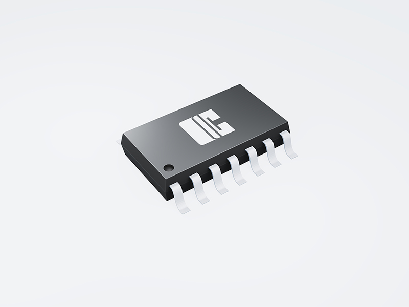
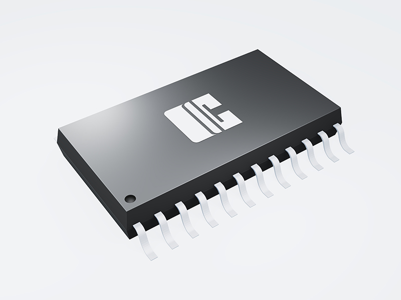
16パッケージ :
DIP16/SOP16/TSSOP16/DHVQFN16-5 V~+5 Vの広いアナログ入力電圧範囲
広い供給電圧範囲
AiP74HC4051: 3V~9V
低オン抵抗:
– 80 Ω(標準)、VCC - VEE = 4.5 V
– VCC - VEE = 6.0 Vで70 Ω(標準)
– 60 Ω(標準)、VCC - VEE = 9.0 V
ロジックレベル変換: 5 Vロジックを±5 Vアナログ信号と通信できるようにする
典型的な「ブレーク・ビフォア・メイク」の組み込み
-40°C~+125°Cの範囲で指定
パッケージ情報: DIP16/SOP16/TSSOP16/DHVQFN16
用途:
アナログ多重化と多重分離
デジタル多重化と多重分離
The AiP74HC/HCT4851 is 8-channel analog multiplexers/demultiplexers with three digital select inputs (S0 to S2), an active-LOW enable input (E—), eight independent inputs/outputs (Y0 to Y7) and a common input/output (Z). The devices feature injection-current effect control, which has excellent value in automotive applications where voltages in excess of the supply voltage are common.
詳細
The AiP74HC/HCT4851 is 8-channel analog multiplexers/demultiplexers with three digital select inputs (S0 to S2), an active-LOW enable input (E—), eight independent inputs/outputs (Y0 to Y7) and a common input/output (Z). The devices feature injection-current effect control, which has excellent value in automotive applications where voltages in excess of the supply voltage are common.
詳細
The AiP74HC/HCT48751 is a single-pole octal-throw analog switch (SP8T) suitable for use in analog or digital 8:1 multiplexer/demultiplexer applications. The switch features three digital select inputs (S0, S1 and S2), eight independent inputs/outputs (Yn), a common input/output (Z) and a digital enable input (E—). When E—is HIGH, the switches are turned off.
詳細
The AiP74HC/HCT48751 is a single-pole octal-throw analog switch (SP8T) suitable for use in analog or digital 8:1 multiplexer/demultiplexer applications. The switch features three digital select inputs (S0, S1 and S2), eight independent inputs/outputs (Yn), a common input/output (Z) and a digital enable input (E—). When E—is HIGH, the switches are turned off.
詳細
The AiP74HC/HCT48752 is a dual single-pole quad-throw analog switch (2×SP4T) suitable for use in analog or digital 4:1 multiplexer/demultiplexer applications. Each switch features four independent inputs/outputs (nY0, nY1, nY2 and nY3) and a common input/output (nZ). A digital enable input (E—) and two digital select inputs (S0 and S1) are common to both switches. When E—is HIGH, the switches are turned off.
詳細
The AiP74HC/HCT48752 is a dual single-pole quad-throw analog switch (2×SP4T) suitable for use in analog or digital 4:1 multiplexer/demultiplexer applications. Each switch features four independent inputs/outputs (nY0, nY1, nY2 and nY3) and a common input/output (nZ). A digital enable input (E—) and two digital select inputs (S0 and S1) are common to both switches. When E—is HIGH, the switches are turned off.
詳細
The AiP74HC/HCT48753 is a triple single-pole double-throw analog switch (3×SPDT) suitable for use in analog or digital 2:1 multiplexer/demultiplexer applications. Each switch features a digital select input (Sn), two independent inputs/outputs (nY0 and nY1) and a common input/output (nZ). A digital enable input (E—) is common to all switches. When E—is HIGH, the switches are turned off.
詳細
The AiP74HC/HCT48753 is a triple single-pole double-throw analog switch (3×SPDT) suitable for use in analog or digital 2:1 multiplexer/demultiplexer applications. Each switch features a digital select input (Sn), two independent inputs/outputs (nY0 and nY1) and a common input/output (nZ). A digital enable input (E—) is common to all switches. When E—is HIGH, the switches are turned off.
詳細
The AiP74LV4051 is a low-voltage CMOS device and is pin and function compatible with the AiP74HC/HCT4051. The AiP74LV4051 is an 8-channel analog multiplexer/demultiplexer with three digital select inputs (S0 to S2), an active-LOW enable input (E), eight independent inputs/outputs (Y0 to Y7) and a common input/output (Z).
詳細
The AiP74LV4052 is a low-voltage CMOS device and is pin and function compatible with the AiP74HC/HCT4052.The AiP74LV4052 is a dual 4-channel analog multiplexer/demultiplexer with a common select logic. Each multiplexer has four independent inputs/outputs (nY0 to nY3) and a common input/output (nZ). The common channel select logics include two digital select inputs (S0 and S1) and an active LOW enable input (E(—)). With E(—) LOW, one of the four switches is selected (low impedance ON-state) by S0 and S1. With E(—) HIGH, all switches are in the high impedance OFF-state, independent of S0 and S1. VCC and GND are the supply voltage pins for the digital control inputs (S0, S1 and E(—)). The VCC to GND ranges are 1.0V to 6.0V. The analog inputs/outputs (nY0, to nY3, and nZ) can swing between VCC as a positive limit and VEE as a negative limit. VCC-VEE may not exceed 6.0V. For operation as a digital multiplexer/demultiplexer, VEE is connected to GND (typically ground).
詳細
The AiP74LV4053 is a triple single-pole double-throw (SPDT) analog switch, suitable for use as an analog or digital multiplexer/demultiplexer.
詳細
The AiP74LV48751 is an 8-channel analog multiplexer/demultiplexer with three digital select inputs (S0 to S2), an active-LOW enable input (E), eight independent inputs/outputs (Y0 to Y7) and a common input/output (Z).
詳細
The AiP74LV48752 is a dual 4-channel analog multiplexer/demultiplexer with a common select logic. Each multiplexer has four independent inputs/outputs (nY0 to nY3) and a common input/output (nZ). The common channel select logics include two digital select inputs (S0 and S1) and an active LOW enable input (E—). With E—LOW, one of the four switches is selected (low impedance ON-state) by S0 and S1. With E—HIGH, all switches are in the high impedance OFF-state, independent of S0 and S1. VCC and GND are the supply voltage pins for the digital control inputs (S0, S1 and E—). The VCC to GND ranges are 2.0V to 6.0V. The analog inputs/outputs (nY0, to nY3, and nZ) can swing between VCC as a positive limit. VCC may not exceed 6.0V.
詳細
The AiP74LV48753 is a triple single-pole double-throw (SPDT) analog switch, suitable for use as an analog or digital multiplexer/demultiplexer.
詳細
The AiP74LVC1G66 provides one single pole, single-throw analog switch function. It has two input/output terminals (Y and Z) and an active HIGH enable input pin (E). When E is LOW, the analog switch is turned off.
詳細
The AiP74LVC1G3157 provides one analog multiplexer/demultiplexer with one digital select input (S), two independent inputs/outputs (Y0, Y1) and a common input/output (Z).Schmitt trigger action at the select input makes the circuit tolerant of slower input rise and fall times across the entire VCC range from 1.65V to 5.5V.
詳細
The CD4051 is an 8-channel analog multiplexer/demultiplexer with three address inputs (S1 to S3), an active LOW enable input (E(—)), eight independent inputs/outputs (Y0 to Y7) and a common input/output (Z). The device contains eight bidirectional analog switches, each with one side connected to an independent input/output (Y0 to Y7) and the other side connected to a common input/output (Z). With E(—) LOW, one of the eight switches is selected (low-impedance ON-state) by S1 to S3. With E(—) HIGH, all switches are in the high-impedance OFF-state, independent of S1 to S3. If break before make is needed, then it is necessary to use the enable input.VDD and VSS are the supply voltage connections for the digital control inputs (S1 to S3, and E(—)). The VDD to VSS range is 3V to 9V. The analog inputs/outputs (Y0 to Y7, and Z) can swing between VDD as a positive limit and VEE as a negative limit. VDD-VEE may not exceed 9V. Unused inputs must be connected to VDD, VSS, or another input. For operation as a digital multiplexer/demultiplexer, VEE is connected to VSS (typically ground). VEE and VSS are the supply voltage connections for the switches.
詳細
The CD4051H is an 8-channel analog multiplexer/demultiplexer with three address inputs (S1 to S3), an active LOW enable input (E(—)), eight independent inputs/outputs (Y0 to Y7) and a common input/output (Z). The device contains eight bidirectional analog switches, each with one side connected to an independent input/output (Y0 to Y7) and the other side connected to a common input/output (Z). With E(—) LOW, one of the eight switches is selected (low-impedance ON-state) by S1 to S3. With E(—) HIGH, all switches are in the high-impedance OFF-state, independent of S1 to S3. If break before make is needed, then it is necessary to use the enable input.VDD and VSS are the supply voltage connections for the digital control inputs (S1 to S3, and E(—)). The VDD to VSS range is 3V to 18V. The analog inputs/outputs (Y0 to Y7, and Z) can swing between VDD as a positive limit and VEE as a negative limit. VDD-VEE may not exceed 18V. Unused inputs must be connected to VDD, VSS, or another input. For operation as a digital multiplexer/demultiplexer, VEE is connected to VSS (typically ground). VEE and VSS are the supply voltage connections for the switches.
詳細
The CD4051HS is an 8-channel analog multiplexer/demultiplexer with three address inputs (S1 to S3), an active LOW enable input (E—), eight independent inputs/outputs (Y0 to Y7) and a common input/output (Z).The device contains eight bidirectional analog switches, each with one side connected to an independentinput/output (Y0 to Y7) and the other side connected to a common input/output (Z). With E—LOW, one ofthe eight switches is selected (low-impedance ON-state) by S1 to S3. With E—HIGH, all switches are in the high-impedance OFF-state, independent of S1 to S3. If break before make is needed, then it is necessary to use the enable input.VDD and VSS are the supply voltage connections for the digital control inputs (S1 to S3, and E—). The VDD to VSS range is 3V to 18V. The analog inputs/outputs (Y0 to Y7, and Z) can swing between VDD as a positive limit and VEE as a negative limit. VDD-VEE may not exceed 18V. Unused inputs must be connected to VDD, VSS, or another input. For operation as a digital multiplexer/demultiplexer, VEE is connected to VSS(typically ground). VEE and VSS are the supply voltage connections for the switches.
詳細
The CD4052 is a dual 4-channel analogue multiplexer/demultiplexer with common channel select logic. Each multiplexer/demultiplexer has four independent inputs/outputs (nY0 to nY3) and a common input/output (nZ). The common channel select logic includes two select inputs (S1 and S2) and an active LOW enable input (E(—)). Both multiplexers/demultiplexers contain four bidirectional analog switches, each with one side connected to an independent input/output (nY0 to nY3) and the other side connected to a common input/output (nZ). With E(—) LOW, one of the four switches is selected (low-impedance ON-state) by S1 and S2. With E(—) HIGH, all switches are in the high-impedance OFF-state, independent of S1 and S2. If break before make is needed, then it is necessary to use the enable input.VDD and VSS are the supply voltage connections for the digital control inputs (S1 and S2, and E(—)). The VDD to VSS range is 3V to 9V. The analog inputs/outputs (nY0 to nY3, and nZ) can swing between VDD as a positive limit and VEE as a negative limit. VDD-VEE may not exceed 9V. Unused inputs must be connected to VDD, VSS, or another input. For operation as a digital multiplexer/demultiplexer, VEE is connected to VSS (typically ground). VEE and VSS are the supply voltage connections for the switches.
詳細
The CD4052H is a dual 4-channel analogue multiplexer/demultiplexer with common channel select logic. Each multiplexer/demultiplexer has four independent inputs/outputs (nY0 to nY3) and a common input/output (nZ). The common channel select logic includes two select inputs (S1 and S2) and an active LOW enable input (E(—)). Both multiplexers/demultiplexers contain four bidirectional analog switches, each with one side connected to an independent input/output (nY0 to nY3) and the other side connected to a common input/output (nZ). With E(—) LOW, one of the four switches is selected (low-impedance ON-state) by S1 and S2. With E(—) HIGH, all switches are in the high-impedance OFF-state, independent of S1 and S2. If break before make is needed, then it is necessary to use the enable input.VDD and VSS are the supply voltage connections for the digital control inputs (S1 and S2, and E(—)). The VDD to VSS range is 3V to 18V. The analog inputs/outputs (nY0 to nY3, and nZ) can swing between VDD as a positive limit and VEE as a negative limit. VDD-VEE may not exceed 18V. Unused inputs must be connected to VDD, VSS, or another input. For operation as a digital multiplexer/demultiplexer, VEE is connected to VSS (typically ground). VEE and VSS are the supply voltage connections for the switches.
詳細
The CD4053 is a triple single-pole double-throw (SPDT) analog switch, suitable for use as an analog or digital multiplexer/demultiplexer. Each switch has a digital select input (Sn), two independent inputs/outputs (nY0 and nY1) and a common input/output (nZ). All three switches share an enable input (E(—)). A HIGH on E(—) causes all switches into the high-impedance OFF-state, independent of Sn.VDD and VSS are the supply voltage connections for the digital control inputs (Sn and E(—)). The VDD to VSS range is 3V to 9V. The analog inputs/outputs (nY0, nY1, and nZ) can swing between VDD as a positive limit and VEE as a negative limit. VDD-VEE may not exceed 9V. Unused inputs must be connected to VDD, VSS, or another input. For operation as a digital multiplexer/demultiplexer, VEE is connected to VSS (typically ground). VEE and VSS are the supply voltage connections for the switches.
詳細
The CD4053H is a triple single-pole double-throw (SPDT) analog switch, suitable for use as an analog or digital multiplexer/demultiplexer. Each switch has a digital select input (Sn), two independent inputs/outputs (nY0 and nY1) and a common input/output (nZ). All three switches share an enable input (E(—)). A HIGH on E(—) causes all switches into the high-impedance OFF-state, independent of Sn.VDD and VSS are the supply voltage connections for the digital control inputs (Sn and E(—)). The VDD to VSS range is 3V to 18V. The analog inputs/outputs (nY0, nY1, and nZ) can swing between VDD as a positive limit and VEE as a negative limit. VDD-VEE may not exceed 18V. Unused inputs must be connected to VDD, VSS, or another input. For operation as a digital multiplexer/demultiplexer, VEE is connected to VSS (typically ground). VEE and VSS are the supply voltage connections for the switches.
詳細
The CD4066 provides four single-pole, single-throw analog switch functions. Each switch has two input/output terminals (nY and nZ) and an active HIGH enable input (nE). When nE is LOW, the analog switch is turned off.The CD4066 is pin compatible with the CD4016 but exhibits a much lower ON resistance. In addition the ON resistance is relatively constant over the full input signal range.
詳細
The CD4094 is an 8-stage serial shift register. It has a storage latch associated with each stage for strobing data from the serial input to parallel buffered 3-state outputs QP0 to QP7. The parallel outputs may be connected directly to common bus lines. Data is shifted on positive-going clock transitions. The data in each shift register stage is transferred to the storage register when the strobe (STR) input is HIGH. Data in the storage register appears at the outputs whenever the output enable (OE) signal is HIGH.Two serial outputs (QS1 and QS2) are available for cascading a number of CD4094 devices. Serial data is available at QS1 on positive-going clock edges to allow high-speed operation in cascaded systems with a fast clock rise time. The same serial data is available at QS2 on the next negative going clock edge. This is used for cascading CD4094 devices when the clock has a slow rise time.It operates over a recommended VDD power supply range of 3V to 15V referenced to VSS (usually ground). Unused inputs must be connected to VDD, VSS, or another input.
詳細
AiP74CBTLV3125 is a 4-bit bus single-channel analog switch circuit. Each bit is controlled by the separate enable port (1OE—to 4OE—) and enable ports are all Schmitt designed. To ensure the high-impedance OFF-state during power-up or power-down, it is recommended that nOE—connect an external pull-up resistor to VCC. When the circuit is in power down state (VCC=0V), the control port and the switch port are in high resistance state, which can effectively prevent backflow and circuit damage.
詳細
AiP74CBTLV3126 is a 4-Bit bus switch circuit. Each bit is controlled by the separate enable port (1OE~4OE) and enable ports are all Schmitt design. To ensure the high-impedance OFF-state during power-up or power-down, it is recommended that nOE connect an external drop-down resistor to GND. When the circuit is in power down state (VCC=0V), the control port and the switch port are in high resistance state, which can effectively prevent backflow and circuit damage.
詳細
AiP74CBTLV3245 is an 8-bit bus switch with output enable. The circuit has a common enable control port (OE—), which is Schmitt designed. To ensure the high-impedance OFF-state during power-up or power-down, it is recommended that OE—connect an external pull-up resistor to VCC. When the circuit is in power down state (VCC=0V), the control port and the switch port are in high resistance state, which can effectively prevent backflow and circuit damage.
詳細
AiP74CBTLV3253 is a dual 1-of-4 multiplexer/demultiplexer. The circuit has two common selection ports (S0, S1) and two enable control ports (1OE , 2OE ). To ensure the high-impedance OFF-state during power up or power down, 1OE and 2OE should be tied toVcc through a pull-up resistor. This device is fully specified for partial power-down applications using IOFF. The IOFFcircuitry disables the output, preventing the damaging backflow current through thedevice when it is powered down.
詳細
AiP74CBTLV3257 is a 4-Bit 1-of-2 FET Multiplexer/Demultiplexer. The circuit has a common selection port (S) and an enable control port (OE(—)).To ensure the high-impedanceOFF-state during power upor power down, OE(—) should be tied to Vcc through apull-up resistor.This device is fully specified for partial power-down applications using IOFF. The IOFF circuitry disables the output, preventing the damaging backflow current through the device when it is powered down.
詳細
AiP74CBTLV3306 is a 2-bit bus switch. The circuit has a common enable control port (OE—), which is designed as a Schmitt trigger. To ensure the high-impedance OFF-state during power up or power down, OE—should be tied to VCC through a pull-up resistor. This device is fully specified for partial power-down applications using IOFF. The IOFFcircuitry disables the output, preventing the damaging backflow current through thedevice when it is powered down.
詳細
AiP74CBTLV3861 is a 10-bit bus switch with output enable. The circuit has a common enable control port (OE -), which is Schmitt designed. To ensure the high-impedance OFF-state during power-up or power-down, it is recommended that (OE -) connect an external pull-up resistor to VCC. When the circuit is in power down state (VCC=0V), the control port and the switch port are in high resistance state, which can effectively prevent backflow and circuit damage.
詳細
AiP74CB3Q3245 is an 8-bit bus switch with output enable and charge pump. A built-in charge pump is used to increase the gate voltage of the NMOS pass transistor, enabling the circuit to transmit 5.5V switching signals when VCC=3.3V.
詳細
AiP74CB3Q3251 is a 1-of-8 multiplexer/demultiplexer with charge pump. The circuit has selection port (S0 to S2) and enable control port (OE -).A built-in charge pump is used to increase the gate voltage of the NMOS pass transistor, enabling the circuit to transmit 5.5V switching signals when VCC=3.3V.
詳細
AiP74CB3Q3253 is a dual 1-of-4 multiplexer/demultiplexer. The circuit has selection port (Sn) and enable control port (nOE—).A built-in charge pump is used to increase the gate voltage of the NMOS pass transistor, enabling the circuit to transmit 5.5V switching signals when VCC=3.3V.
詳細
AiP74CB3Q3257 is a 4-bit 1-of-2 multiplexer/demultiplexer. The circuit has common select port (S) and enable control port (OE—).A built-in charge pump is used to increase the gate voltage of the NMOS pass transistor, enabling the circuit to transmit 5.5V switching signals when VCC=3.3V.
詳細
AiP74CB3Q3245 is a dual bus switch with charge pump. A built-in charge pump is used to increase the gate voltage of the NMOS pass transistor, enabling the circuit to transmit 5.5V switching signals when VCC=3.3V.
詳細
AiP74HC4051は、アナログまたはデジタル8:1マルチプレクサ/デマルチプレクサアプリケーションに適した単極8投アナログスイッチ(SP8T)です。このスイッチは、3つのデジタルセレクト入力(S0、S1、S2)、8つの独立した入出力(Yn)、共通入出力(Z)、およびデジタルイネーブル入力(E—)を備えています。
詳細
AiP74HCT4051は、アナログまたはデジタル8:1マルチプレクサ/デマルチプレクサアプリケーションに適した単極8投アナログスイッチ(SP8T)です。このスイッチは、3つのデジタルセレクト入力(S0、S1、S2)、8つの独立入出力(Yn)、共通入出力(Z)、およびデジタルイネーブル入力(E—)を備えています。
詳細
AiP74HC4052は、デュアル単極4投アナログスイッチ(2×SP4T)で、アナログまたはデジタル4:1マルチプレクサ/デマルチプレクサアプリケーションに適しています。各スイッチは、4つの独立した入出力(nY0、nY1、nY2、nY3)と1つの共通入出力(nZ)を備えています。デジタルイネーブル入力(E—)と2つのデジタルセレクト入力(S0、S1)は、両方のスイッチに共通です。
詳細
AiP74HCT4052は、デュアル単極4投アナログスイッチ(2×SP4T)で、アナログまたはデジタル4:1マルチプレクサ/デマルチプレクサアプリケーションに適しています。各スイッチは、4つの独立した入出力(nY0、nY1、nY2、nY3)と1つの共通入出力(nZ)を備えています。デジタルイネーブル入力(E—)と2つのデジタルセレクト入力(S0、S1)は、両方のスイッチに共通です。
詳細
AiP74HC4053は、アナログまたはデジタル2:1マルチプレクサ/デマルチプレクサアプリケーションに適した、トリプル単極双投アナログスイッチ(3×SPDT)です。各スイッチは、デジタルセレクト入力(Sn)、2つの独立した入出力(nY0とnY1)、および共通入出力(nZ)を備えています。
詳細
AiP74HCT4053は、アナログまたはデジタル2:1マルチプレクサ/デマルチプレクサアプリケーションに適した、トリプル単極双投アナログスイッチ(3×SPDT)です。各スイッチは、デジタルセレクト入力(Sn)、2つの独立した入出力(nY0とnY1)、および共通入出力(nZ)を備えています。
詳細
AiP74HC4066は、4つの単極単投アナログスイッチです。各スイッチは、2つの入出力端子(nYとnZ)とアクティブHIGHのイネーブル入力(nE)を備えています。nEがLOWのとき、アナログスイッチはオフになります。。
詳細
AIP74HC/HCT4097は、3つのバイナリ制御入力A0、A1、A2と1つのインヒビット入力(E—)を備えた差動8チャネルマルチプレクサです。これらの入力により、8組のスイッチから1つを選択できます。
詳細

伝言を残す